As a part of my search for a thesis topic I've been researching quantum dot solar cells along with other various solar-electric technologies. I thought I would share some of my results. I hope this post is not too technical; please feel free to comment away. I've tried to define terms that I don't think will be too familar, and have included a number of Wikipedia links.
Introduction to Solar Power
Photovoltaic device is the proper term for a solar-electric cell than collects sunlight (otherwise known as
insolation) and converts it to electricity. The dominate technology in use in the photovoltaic world is phosphorous and boron (or aluminium) doped poly-crystalline silicon wafers approximately 0.3 mm thick. They convert insolation to electricity at approximately 13 % efficiency.
The production of electricity from photovoltaic devices is currently uneconomical compared to fossil fuel or nuclear sources except for applications located off the electrical grid. For example, the largest single use of photovoltaic devices in Canada is to power monitoring equipment for oil and gas wells. Furthermore the production of power from photovoltaic devices is intermittent. The amount of power they generate varies depending on the angle of the sun in the sky throughout the day and clouds have a deleterious effect by diffusing the sunlight. The electrical needs of society cannot be met purely through solar power alone without substantial investment in energy storage, voltage regulation, and load following infrastructure. As such solar power represents a component in the future power mix, but it is unlikely to be the sole source of energy.
The high cost associated with electricity derived from photovoltaics is due to their low efficiency, high materials cost of ultra-pure
zone refined silicon, and the thick substrate necessary for a indirect band-gap material necessary to absorb as much as the incident radiation as possible. The fundamental need for photovoltaics to become competitive as power producers compared to conventional is reduced cost by reducing the materials cost, reducing infrastructure and time needed for manufacture, and improving the efficiency. Nanoscale structures including quantum dots have the potential to improve both the efficiency and cost of photovoltaics through a variety of means.
Photovoltaic Operation
A photovoltaic device needs to fulfill two basic parameters: it needs to generate free charge carriers through interaction with a photon flux and then it needs to separate the charge carriers and generate an electrical current before they can decay from their excited state (or recombine) [
1].
Bandgap: In semiconductors there are two main energy levels (or bands) that electrons may occupy: the valence band and the conduction band. At absolute zero all the electrons will be in the valence band and unable to move and hence conduct electricity. As temperature rises the population in the conduction band rises and these promoted electrons act as charge carriers. Similarly the absence of electrons in the valence band -- known as holes -- act as virtual positive charge carriers. Photons with energy greater than the bandgap can be absorbed by electrons in the valence band, promoting them to the conduction band. This is known as electron-hole pair generation and is the basis for photovoltaic operation.
Doping: Intrinsic semiconductors such as Silicon are often intentionally doped with contaminants to change their electronic properties. Doping can introduce either a surplus of negative charge carriers (electrons) in n-type doping or a surplus of positive charge carriers (holes) in p-type doping.
The standard method to achieve this is through a p-type doped Silicon wafer with a thin n-layer deposited on the surface, i.e. a p-n junction [Figure 1]. The electronic mismatch between the n and p-doped regions generates a potential bias across the transistor and results in electrons and holes gathered on their respective surfaces. The intermediate region is depleted of charge carriers – hence the term depletion region. When under illumination the absorption of photons creates a higher density of charge carriers and the potential bias becomes stronger. In general, the stronger the electric field the faster charge carriers will be swept out to their respective terminals.
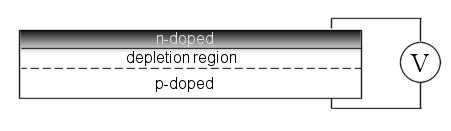 Figure 1: A standard photovoltaic device with a p-doped base semiconductor and a thin n-doped surface region (which is usually patterned to reduce reflection losses and better trap light). The depletion region is devoid of charge carriers due to the high density of electrons on the surface and holes of the base material.
Whenever an electron-hole pair is able to decay from its excited state back to the valence band there is a loss of exergy from the system with a corresponding reduction in efficiency. Electron-hole pairs can radiatively recombine, whereby they emit a photon. In Auger recombination an electron-hole pair gives up its energy to another excited electron, moving it to a higher state. These two processes are intrinsic physical processes and cannot be avoided; they can only be minimized by sweeping out the charge carriers to the electrodes quickly. Auger recombination is however dependent on the preexistence of electrons in the conduction band, and hence is dependent on excitation and doping levels. Recombination can also occur at crystal grain boundaries and trap sites in material. These processes are thermal and can be reduced through better quality control in manufacturing.
There are electrical contacts located on the front and back of the cell that allow charge to be removed. There are a variety of electrical engineering issues associated with the design and optimization of photovoltaic cells that I will not discuss in this post.
Solar Spectrum
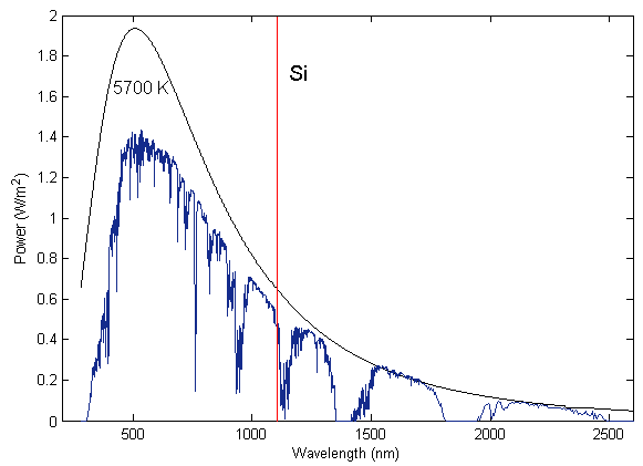
The sun can be approximated as a black body at 5760 K with an irradiance of 1400 W/m
2 at one astronomical unit distance. The peak wavelength is usually 503 nm (2.45 eV), but varies with solar weather. Due to a variety of absorption and scattering processes the spectrum observed on the Earth's surface is significantly different. The total irradiance is attenuated and there are a number of absorption valleys. In order to standardize the performance of photovoltaic devices researchers have devised a standard solar spectrum known as the Air Mass 1.5 standard [
2]. The Air-Mass 1.5 standard is intended to mimic a mean characteristic spectrum for the USA at a power density of 1000 W/m
2.
Electron Volt (eV): The energy a electron gains by passing through a potential of 1 Volt which is 1.602 x 10⁻¹⁹ Joules. A photon with wavelength 1240 nm (infrared) has an energy of 1.0 eV.
Photons emitted by the sun have a wide distribution of energies [Figure 2]. Any photovoltaic device should be optimized to collect the spectrum with high efficiency. For a single band-gap material, this is not especially easy. Photons with less energy than the band-gap cannot generate electron-hole pairs and hence will be wasted. For photons with greater energy than the band-gap, the photon will only be able to generate one electron-hole pair at a fixed potential difference so the excess energy is lost. For a material with a band-gap of 1.1 eV, the maximum efficiency can be shown to be 30 %, and the optimum band-gap of 1.4 eV has a maximum efficiency of 33 % [
3]. This is a slightly simplified case.
 Figure 2: The Air Mass 1.5 spectrum compared to a 5700 K blackbody radiator. The red line represents Silicon's band-gap. The infrared absorption regions are from dipole molecules such as CO2 and water in the atmosphere.
Methods for Improved Efficiency
In order to improve the efficiency beyond that of a single band-gap material there are a variety of strategies that may be employed, namely:
- To employ materials of different band-gap to absorb different wavelengths, through stacking or some other arrangement.
- The process converting high energy photons to multiple electron-hole pairs is known as down conversion. One possible process is by impact ionization.
- The process of converting low energy photons into a single electron-hole pair is known as up conversion. One possible method to achieve this is by introducing an intermediate (exciton) state in the forbidden region to all two photons to promote an electron from the valence band in a step-wise fashion.
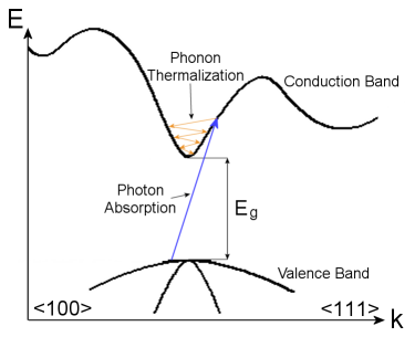
Methods 1 and 2 act to reduce the losses through thermalization of ‘hot’ electrons [Figure 3]. Essentially, multiple band-gap materials allow for extra absorption lines to be drawn on the solar spectrum. Impact ionization allows the better utilization of shorter wavelengths while two-photon absorption allows utilization of longer wavelengths in the generation of photocurrent.
 Figure 3: A direct band-gap material absorbs a photon with energy greater than its band-gap. Subsequently the generated electron-hole pair will thermalize via phonon emission to the lowest available energy level in the band. The momentum of the photon and energy of the phonons has been exaggerated.
There are a number of other methods to improve efficiency that will not be covered here. One of the greatest sources of electron-hole recombination in commercial solar cells is at defect sites created by impurities. For comparison, while monocrystalline silicon cells in the laboratory have achieved an efficiency of 27 % commercial units rarely top 16 % [
1]. Reducing the losses due to surface reflection is also important. Most semiconductors have high indices of refraction which imply a high natural reflection with an air interface. This reflection can be reduced by various anti-reflection coatings. Surface patterning also plays a role in reducing the reflectance of cells at glazing incidence.
Quantum Dots and Applications to Photovoltaics
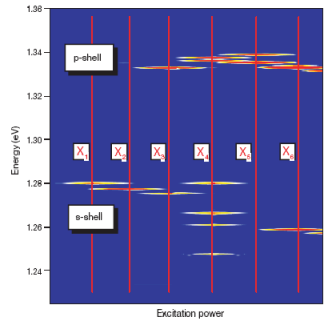
Quantum dots are pseudo-zero dimensional structures. They typically are represented as small clusters of several hundred atoms with a diameter of 5 nm or less. The small physical dimensions of quantum dots act to restrict the wave function of electrons and holes. This is known as quantum confinement and it acts to increase the energy of electrons and holes located inside the quantum dot. The quantum dot acts as a potential well, increasing the potential energy of an electron or hole caught inside. Quantum dots can be considered artificial atoms because it has been shown that they form excitonic electronic levels that are analogous to the s and p orbitals of elements Hydrogen through Carbon [
4,
5]. This can be seen clearly in [Figure 4], where the number of emission lines corresponding to energy levels increases with applied power.
Exciton: An exciton is an electron and hole that are bound together rather than being free to roam around. Since holes typically have a much greater effective mass than electrons in a material one can think of an exciton as being analogeous to hydrogen, with the hole taking the place of the proton.
 Figure 4: In0.6Ga0.4As quantum dot emission spectrum as a function of applied power. Notice that the energy spread of the lines is very narrow [4].
Quantum dots, through quantum confinement, act as a means of tailoring the energy bands that are available for electron-hole pairs, limiting the wavelengths of light they can couple to. In essence, the
density of states for a quantum dots only allows very specific energy levels. In a system of quantum dots the allowed energy levels is slightly broadened by the non-uniformity of the dots’ dimensions. If the energy bands in quantum dots are sufficiently separated (~ 50 meV), the probability of thermalization between the bands is low because individual phonons lack the requisite energy for a transition.
Phonon: A phonon is a quantum mechanical representation of vibration of a solid's crystal lattice. Essentially they are quata of heat. At 300 K (about room temperature) phonons have an average energy of 25 meV.
Quantum dots offer an easy method to vary their band-gap through variation of their physical dimensions. They may also be able to achieve impact ionization with much greater quantum efficiency than bulk semiconductors. The use of tailored energy level quantum dots may also allow their use as intermediate bands in up conversion photovoltaics. Quantum dots can be fabricated through a variety of means but molecular beam epitaxy is the most common for semiconductor applications [
6].
Multiple Band Gaps through Quantum Dots
A common scheme to improving the work done per photon in solar cells is to stack junctions of increasing band gap on top of each other. Practically only two or three junctions may be stacked. The introduction of nanostructures potentially allows for a greater number of energy gaps to be introduced through quantum confinement. With an infinite number of band-gaps available the maximum theoretical efficiency of photovoltaics is 69 % [
1].
The earliest work on multiple band-gap photovoltaics involving nanostructures was regarding the use of quantum wells [
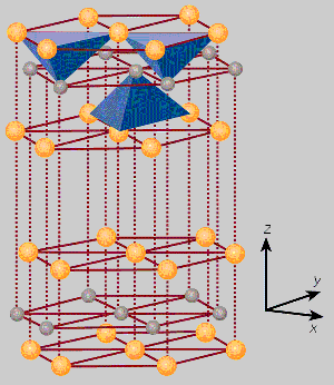
7]. Aroutiounian et al. have suggested that quantum dots could be placed in a thick intrinsic region of a n-i-p hetrojunction [
8]. The authors propose using a GaAs/InAs structure since it can generate a variety band-gaps well matched to the solar spectrum. Aroutiounian suggest epitaxy as a growth mechanism using the phenomenon of self-assembly through lattice mismatch strain. Furthermore, if the quantum dots are stacked closely enough, the strain fields of the lower dots will extend through the bulk substrate which encourages quantum dots to vertically align themselves into columns [Figure 5]. In essence, the quantum dots are encouraged to form into weak quantum wires; this of critical importance due to the need to extract charge carriers in order to generate photocurrent. Coupling between the quantum dots allows the generated electrons and holes to be injected from the high absorption quantum dots into the n and p regions. The theoretical model of this system demonstrates a 5.5 % improvement in efficiency over the same system without the inclusion of quantum dots.
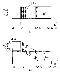 Figure 5: (a) Schematic of arrangement of self-assembled quantum dots in a p-i-n junction and (b) the associated band structure [8].
The man drawback of this methodology would appear to be the need for extensive
molecular beam epitaxy (MBE). The process is slow and hence expensive. It also does not reduce the volume of refined material required for manufacture.
Down Conversion through Impact Ionization with Quantum Dots
Impact ionization is essentially the inverse of the Auger recombination process. In impact ionization a photon with energy greater than twice the band-gap creates an electron-hole pair with considerable excess energy. Normally the electron would then thermalize through phonon emission back to the bottom of the conduction band. However, it is possible also for the electron to relax by generating another electron-hole pair instead. In this manner is it possible to generate more than one free carrier per photon, resulting in greater photocurrent. The resulting product of two electron-hole pairs is sometimes known as a biexciton [Figure 6].
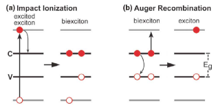
Figure 6: (a) Schematic depiction of impact ionization of a high-energy electron-hole pair and (b) its inverse process, Auger recombination [
10].
Nozik originally proposed that impact ionization might be enhanced in semiconductor nanocrystals [
9]. This was later shown experimentally by Schaller and Klimov [
10]. While impact ionization requires photons with a minimum energy of at least twice the band-gap, the process occurs most frequently at photons with even higher energy. For the PbSe nanocrystals studied by Schaller and Klimov the onset was not seen until E ~ 3 E
g. The peak internal efficiency found was 118 % for photons with energy of 3.8 Eg. (External quantum efficiency is the measured energy efficiency from the current-voltage produced outside the device; internal (quantum) efficiency is the probability of a photon creating an electron-hole pair. For impact ionization internal quantum efficiency can be greater than 100 %.)
Construction of a working photovoltaic prototype with improved performance through impact ionization or some other down conversion method has not yet been achieved. The proof of principle will require demonstrating that the electron-hole pairs generated by the nanocrystals can be extracted to provide electrical current. This may be difficult because the relaxation time of electron-hole pairs generated through this method is very short. While regular electron-hole pairs in the PbSe nanocrystals were shown to have a relaxation time on the order of a microsecond, the so called biexciton created through impact ionization tends to decay via Auger recombination on the picosecond scale. If this occurs then the system returns to its original state with one high-energy electron hole pair.
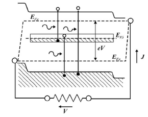
Up Conversion through Quantum Dot Generated Intermediate Band States
Marti et al. have discussed the possibility of engineering quantum dots with distinct energy levels inside the forbidden band gap of a bulk semiconductor p-n junction [
11][
12]. The generation of intermediate (excitonic) energy levels in the band-gap allows for the possibility of the generation of carriers from the absorption of two photons. Because the density of states for quantum dots is so narrow the possibility of thermalization from the intermediate states is avoided.
By carefully tailoring the dimensions of the quantum dots it is possible to engineer their energy levels to occupy intermediate states – typically very near the Fermi level of the intrinsic semiconductor – inside the band-gap [Figure 7]. The structure the authors suggest is an Al
0.4Ga
0.6As (1.95 eV) matrix with 4 nm radius In
0.58Ga
0.42As (0.87 eV) quantum dots spaced in a regular three-dimensional lattice.
 Figure 7: Simplified band-gap for quantum dot intermediate-state n-i-p cell [12].
It is also, however, necessary to balance the population of the intermediate states so that in thermal equilibrium the states are roughly half-full. This requires n-doping of the quantum dots but the authors are unable to suggest an appropriate substitutional donor without relaxation of some of the criteria for optimized efficiency. It can also be seen that the structure is capable stimulated emission if the population in the conduction band is too large.
Thermalvoltaics in Conjugated Polymers with Quantum Dots
Absorption of low energy photons in the near infrared portion of the spectrum (800 – 2000 nm) is the field of thermal photovoltaics (or thermalvoltaics). In this regime there is less power available from the solar spectrum. Generally thermal photovoltaics are envisioned as being paired with visual spectrum photovoltaics in a multiple band-gap structure. It is seen as a challenge to harvest the power available in the infrared economically.
One potentially low cost approach for thermalvoltaics has been examined by Sargent et al. [
13]. Their study was orientated around the use of PbS nanocrystals embedded in
conjugate polymers. The advantage of this technique is the low embedded energy involved in the synthesis of the nanocrystals. They can be prepared in large batches in solution requiring temperatures of only 150 ºC to react PbO and the polymer sulfur source [
14]. Together with the low cost of the base materials one may infer that these quantum dot structures may be fabricated in large quantities very inexpensively.
The minimum band-gap for PbS structures is 0.41 eV (3024 nm) for the bulk material. Through quantum confinement the band-gap for individual PbS nanocrystals this can be increased. In this case the quantum dots are on the order of 20 nm or in radius. A diameter of 6.5 nm corresponds to a structure with an absorption peak at 1300 nm.
The efficiency reported by Sargent is three orders of magnitude greater than previous results using nanostructures for near infrared electro-optical applications. While this may represent a large improvement over previous results the overall performance is still very poor. For an input of 207 mW the photocurrent was 90.61 μA at 5 V, corresponding to an external efficiency of 0.22 %. Compared to solid-state systems, the efficiency is still two orders of magnitude lower. The devices also have the unusual property that efficiency increases under lower irradiance. According to Sargent, the route to achieving practical efficiency for PbS quantum dots lies in improving the conjugate polymer structure and its coupling to the embedded quantum dots along with better light trapping strategies to improve absorption:
Photodetector quantum efficiencies and photovoltaics power efficiencies will benefit from a stronger internal impetus towards rapid charge separation prior to recombination. Short ligands, conducting ligands, and the removal of insulating ligands in favor of direct polymer-nanocrystal contacts will aid in this process, as will the use of smaller ionization-potential polymers. External quantum efficiencies will be enhanced by increasing the effective optical density at the exciton peak through increased nanocrystal loadings and increased interaction lengths via a combination of thicker nanotextured active layers and the use of resonant cavity structures.
Conclusions
Quantum dots and other nanostructures appear to be an excellent means to create tailored energy levels to better leverage the solar spectrum. Where they seem to fail is their adherence to the “keep it simple” principal of engineering. Some of the proposed structures appear to be overly complicated and require excessive quality control on the size and placement of quantum dots. Given that quantum dots are usually on the order of ‘hundreds’ of atoms this seems to pose serious practical issues. Essentially these are photovoltaic systems designed by physicists rather than engineers.
Overall I would not expect any immediate results from quantum dot photovoltaics.
Also, quantum dots on the hole [sic] have difficultly separating the electron and hole from their bound excitonic state. This is a fundamental issue, because the basis of the quantum dot energy levels is the generation of quantum states for excitons through quantum confinement.
Of the solid-state inorganic proposals, the work by Marti on the intermediate band quantum dot solar cell appears to be the most promising. It essentially offers to generate multiple band-gap equivalence through the use of quantum dots embedded in a p-i-n junction. This concept benefits from the long time for radiative recombination in quantum dots because it allows more time for a second incident photon to be absorbed. At the same time, by elevating electron-hole pairs out of the quantum dot excitonic state it side-steps the issues of photocurrent generation.
The work by Sargent is promising but it does not offer to solve many of the problems of all π-conjugated conductive polymer systems: they break down on exposure to UV light and they don’t form protective barriers against oxidation. However, the low energy inputs required for their manufacture compared to conventional semi-conductor photovoltaics is very attractive.
References
1. Nelson, J. (2003). The Physics of Solar Cells London, Imperial College Press.
2. NREL Staff. Reference Solar Spectral Irradiance: Air Mass 1.5, www:http://rredc.nrel.gov/solar/spectra/am1.5/.
3. Shockley, W. and H. J. Queisser (1961). "Detailed Balance Limit of Efficiency of p-n Junction Solar Cells." Journal of Applied Physics 32(3): 510-519.
4. Bayer, M., O. Stern, et al. (2000). "Hidden symmetries in the energy levels of excitonic `artificial atoms'." Nature 405(6789): 923-926.
5. Gammon, D. (2000). "Semiconductor physics: Electrons in artificial atoms." Nature 405(6789): 899-900.
6. Franchi, S., G. Trevisi, et al. (2003). "Quantum dot nanostructures and molecular beam epitaxy." Progress in Crystal Growth and Characterization of Materials 47(2-3): 166-195.
7. Barnham, K. W. J., I. Ballard, et al. (2002). "Quantum well solar cells." Physica E: Low-dimensional Systems and Nanostructures 14(1-2): 27-36.
8. Aroutiounian, V., S. Petrosyan, et al. (2001). "Quantum dot solar cells." Journal of Applied Physics 89(4): 2268-2271.
9. Nozik, A. J. (2002). "Quantum Dot Solar Cells." Physica E 14: 115-120.
10. Schaller, R. D. and V. I. Klimov (2004). "High Efficiency Carrier Multiplication in PbSe Nanocrystals: Implications for Solar Energy Conversion." Physical Review Letters 92(18): 186601-1-4.
11. Marti, A., L. Cuadra, et al. (2000). Quantum Dot Intermediate Band Solar Cell. Photovoltaic Specialists Conference, IEEE.
12. Marti, A., N. Lopez, et al. "Novel semiconductor solar cell structures: The quantum dot intermediate band solar cell." Thin Solid Films In Press, Corrected Proof.
13. McDonald, S. A., G. Konstantatos, et al. (2005). "Solution-processed PbS quantum dot infrared photodetectors and photovoltaics." Nature Materials 4: 138-142.
14. Sargent, E. H. (2005). "Infrared Quantum Dots." Advanced Materials 17(5): 515-522.
 Figure 1: Efficiency versus load for gas turbine.
 Figure 2: Turbine power output versus wind speed. Cuts out at about 4 m/s and feathers at 260 kW and 18 m/s.
 Figure 3: Hourly turbine output for two weeks in March (click to see larger image).
 Figure 4: False-colour graph of wind power output as a function of time and date.
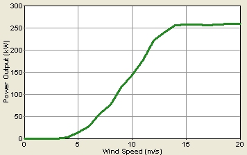 Figure 2: Turbine power output versus wind speed. Cuts out at about 4 m/s and feathers at 260 kW and 18 m/s.
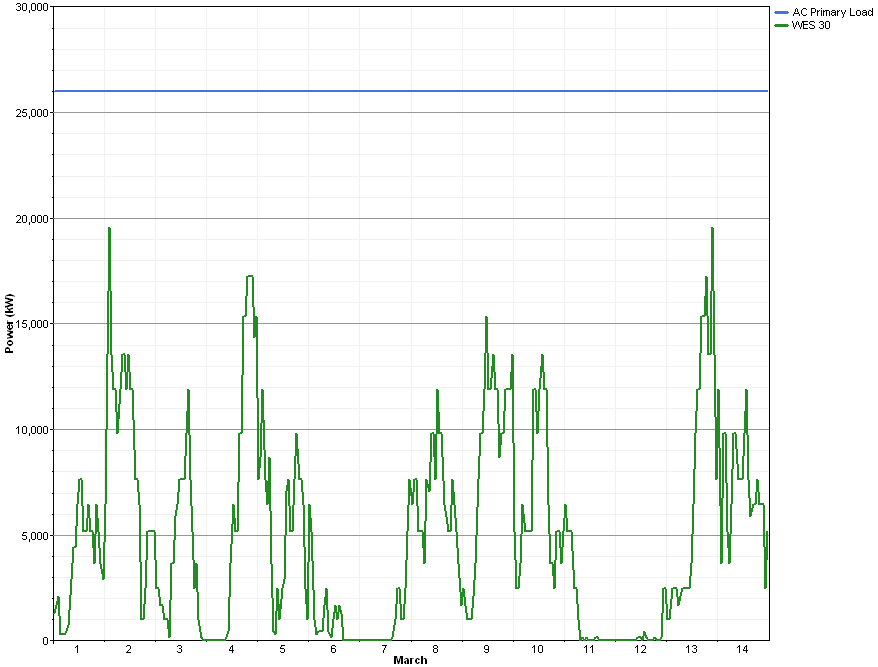 Figure 3: Hourly turbine output for two weeks in March (click to see larger image).
 Figure 4: False-colour graph of wind power output as a function of time and date.